
From 182+X to 2382×1134: Why Did Module Sizes End Up Converging "by Tacit Agreement"?
In brief
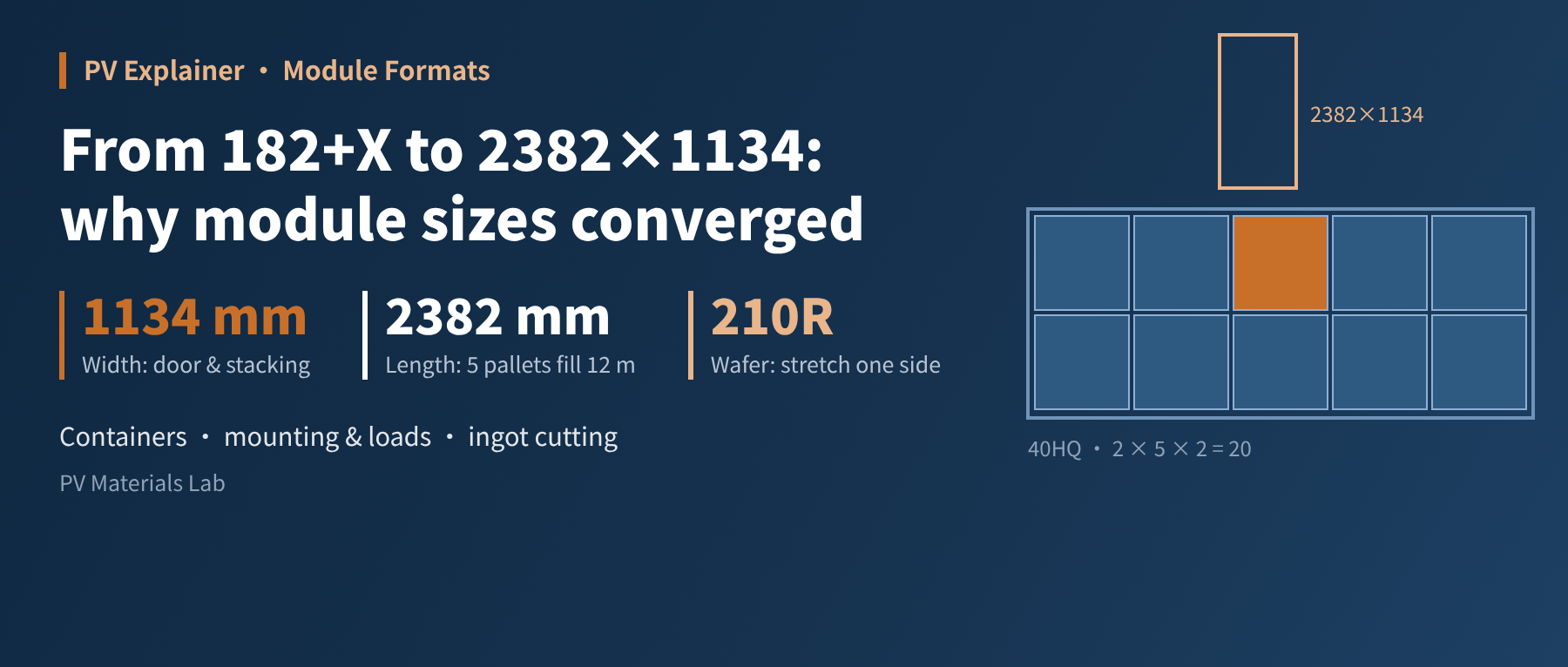
Width fixed at 1,134 mm, length settling around 2,382 mm: the convergence of mainstream module formats was not an arbitrary industry convention but the optimum set by three hard boundaries: the 40-foot high-cube container, mounting structures and mechanical loads, and the cutting of silicon ingots. We work through all three, and explain why a mere "initiative" was enough to bring the whole industry to the same point.
From 156 to 166, from 182 to 210, and on to each company's own "182+X" rectangular wafers, PV module sizes once changed almost every year. Yet by around 2023 the industry had, as if by agreement, converged on a handful of "standard faces": 2382×1134 mm, 2278×1134 mm, 2384×1303 mm and a few others. Nobody decreed this; it was "calculated" by three hard boundaries: containers, mounting structures and silicon ingots. In this article we work through the numbers.
01Meet the few "standard faces" that remain
Conclusion first. In utility-scale and large commercial projects today, these are the formats that keep coming up in quotes, tenders and designs:
| Format (mm) | Wafer | Cell layout | Typical application |
|---|---|---|---|
| 2382×1134 | 210R rectangular 182.2×210 | 66 cells (132 half-cells) | Mainstream mid-size for utility and C&I |
| 2278×1134 | 182 square 182.2×182.2 | 72 cells (144 half-cells) | Previous mainstream; many existing projects |
| 2384×1303 | 210 square 210×210 | 66 cells (132 half-cells) | Large format for big utility plants |
| 1722 / 1762×1134 | 182-series square / rectangular | 54 cells (108 half-cells) | Small format for residential and distributed |
Table 1 Current mainstream module formats
Look closely and a pattern emerges: apart from the large 210 format, almost every format has its width fixed at 1,134 mm. Only the length varies, and the length has settled around 2,382 mm.
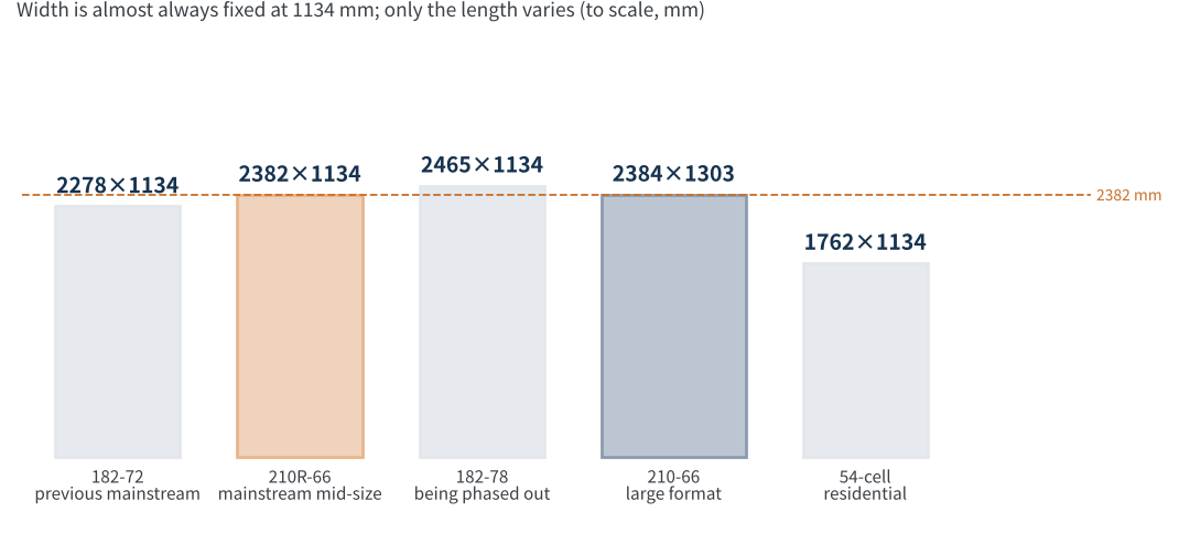
Figure 1 Comparison of mainstream module formats (to scale)
Why can't the width change? And why did the length stop exactly here? The answers lie in three places that seem to have nothing to do with cell technology.
02The first hard boundary: a 40-foot high-cube container
PV is a highly globalised product. Chinese modules travel to Europe, the Middle East and Latin America mostly by sea, and the basic unit of sea freight is the 40-foot high-cube container (40HQ). Its internal dimensions are about 12.03 m long, 2.35 m wide and 2.69 m high, with a door opening that is lower still, about 2.57 m. This box existed long before the PV industry, and its dimensions are a "ceiling" modules must obey.
Modules are usually packed on edge, long side down and short side up, which makes them less prone to micro-cracks from transport vibration. A pallet of modules is about as tall as the module width plus the pallet base. To fill a container, two pallets must be stacked on top of each other, so:
- Width sets the upper limit: two stacked pallets must not exceed the roughly 2.57 m door opening, with about 10 cm left for forklift unloading. Working backwards gives a maximum module width of about 1.13 m. That is where 1,134 mm comes from, and it is also the logic by which the 182 mm wafer (6 columns × 182 mm) was derived in the first place.
- Length is about divisibility: the container is about 12.03 m long inside, and a pallet is about the module length plus a dozen or so millimetres of packaging. Five pallets fill 12 m exactly; any longer and only four fit.
- The awkwardness of the large 210 format: at 1,303 mm wide, two stacked pallets are too tall, so modules must be loaded upright instead, a handling method many customers dislike.
Here is how the 1,134 mm-wide formats fit (see the calculation notes at the end):
| Format (mm) | Pallet length (est.) | Pallets per row | Length utilisation | Pallets per container |
|---|---|---|---|---|
| 2278×1134 | ≈2,292 mm | 5 | ≈95% | 20 |
| 2382×1134 | ≈2,396 mm | 5 | ≈99.6% | 20 |
| 2465×1134 | ≈2,479 mm | 4 | ≈82% | 16 |
Table 2 Estimated 40HQ loading
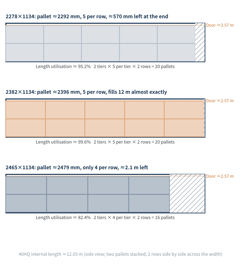
Figure 2 40HQ loading: why 2,382 mm
The result is plain: 2,382 mm is almost exactly the maximum length that still lets five pallets fill 12 m. With the same 20 pallets, the 2382 format carries about 4.6% more module area than the 2278 format, equivalent to 4–5% more watts per container. According to SolarQuarter, Trina's published 210R packaging data are 2,396 × 1,125 × 1,259 mm per pallet, with 20 pallets per 40HQ, 98.5% container utilisation and a 5.4% increase in load. The former 2,465 mm long format overshot the tipping point, fitting only four pallets per row, and its shipping economics dropped sharply.
The 1,134 mm width is set by the door height and two-pallet stacking; the 2,382 mm length is set by the 12 m container length and five pallets per row. The optimal module size is first and foremost a logistics problem.
03The second hard boundary: mounting structures, glass and mechanical loads
Once on site, modules are mounted on structures and must work for more than 25 years. Here too there are boundaries that cannot easily be crossed.
First, mounting holes. Purlins, clamps and hole positions on fixed structures and trackers are designed as a system. The July 2023 initiative by nine companies not only standardised the 2382×1134 size but also unified the longitudinal hole spacing on the long side: 400 mm / 790 mm / 1,400 mm. Unified holes mean structure makers, tracker makers and installers all work with one defined interface. Whether a new format is accepted downstream often depends less on how much more power it has than on whether it "fits".
Second, mechanical loads. A module is essentially a glass plate supported on four sides. The wider it is, the more it deflects in the middle under the same wind and snow load, and the higher the risk of cell cracks and power loss. Industry white-paper calculations show that once module width exceeds 1.2 m, deformation under load causes significant cracking and power loss. Widening a module means thicker glass and stronger frames, adding cost and weight.
Third, glass and other materials. The furnace and line widths of PV rolled glass, and the way raw sheets are cut, are closely tied to the 1,134 mm width. Keeping the width unchanged means cutting specifications for glass, frames, encapsulants and backsheets need no major changes.
- Trackers: with single-module portrait mounting (1P), module length sets the height of each row and its wind area; overly long modules push up the structural cost of the torque tube and drives.
- Strings: a format change alters module voltage and current, affecting the number of modules per string in 1,500 V systems and the inverter configuration.
- Installation: larger, heavier modules affect manual handling, installation pace and breakage rates.
What the downstream fears most is not low power, but "a new format means redoing the whole mounting system and installation method". Keeping the width and hole positions unchanged is the greatest respect for the downstream ecosystem.
04The third hard boundary: a round silicon ingot
The first two boundaries set the module's "outer frame"; the third decides "what goes inside".
Monocrystalline ingots are cylindrical, but cells need to be square or rectangular. Cutting wafers from a round cross-section trims off edge material. That material can be remelted, but re-pulling crystals costs energy and money. To reduce edge waste, wafers are often made as chamfered "pseudo-squares", with an ingot diameter smaller than the wafer diagonal. Using published dimensions, we calculated the area utilisation of several wafer sizes on the ingot cross-section:
| Wafer (mm) | Ingot diameter | Wafer area (est.) | Cross-section utilisation (est.) |
|---|---|---|---|
| M10 182.2×182.2 | Φ247 | ≈331 cm² | ≈69% |
| Rectangular 182.2×191.6 | Φ262.5 | ≈349 cm² | ≈64.5% |
| 210R 182.2×210 | No common published value | ≈383 cm² | — |
| G12 210×210 | Φ295 | ≈441 cm² | ≈64.5% |
Table 3 Estimated ingot cross-section utilisation for different wafer sizes
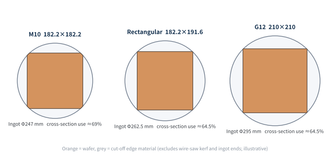
Figure 3 Area utilisation of different wafers on the ingot cross-section (illustrative)
This may run against many people's intuition: rectangular wafers gain nothing when it comes to "cutting a square out of a circle". M10 has higher utilisation because of its larger chamfers: it accepts a missing corner on each side of the wafer in exchange for less edge waste. Rectangular wafers and G12 are cut almost full-square, so cells are more complete and modules have less blank space, but an extra ring of edge material has to be remelted.
So where is the value of rectangular wafers? They let the industry keep enlarging wafer area without touching the 1,134 mm width. Keeping 182.2 mm in one direction means equipment designed around cell width, such as screen printers, PECVD graphite boats and stringers, remains largely compatible; stretching only the other side raises wafer area from about 331 cm² to about 349 cm² or even about 383 cm², spreading the per-piece cost of every slicing, cell and module step.
The question was "how much to stretch". Around 2022, companies successively produced 182×183, 182×185 and 182×188, with plans for 182×192, each only a few millimetres apart. For crystal growers, every size means a different ingot diameter and hot zone; for glass, frame, encapsulant and backsheet makers, every module length means another cutting spec and another inventory. A few millimetres' difference means the supply chain has to stock another set of materials. So in August 2023, six companies (Canadian Solar, Risen, LONGi, Tongwei, DAS Solar and Astronergy) reached a consensus on standardising the rectangular wafer for the 72-cell format, with 182.2 × 191.6 mm and a 262.5 mm ingot diameter becoming the common industry spec, while the 2382×1134 mid-size format is based mainly on the 182.2×210 210R wafer.
Wafer cutting decides "how much bigger you can go within the 1,134 mm frame"; standardisation solves "stop differing by a few millimetres each".
05Why "tacit agreement" rather than "command"
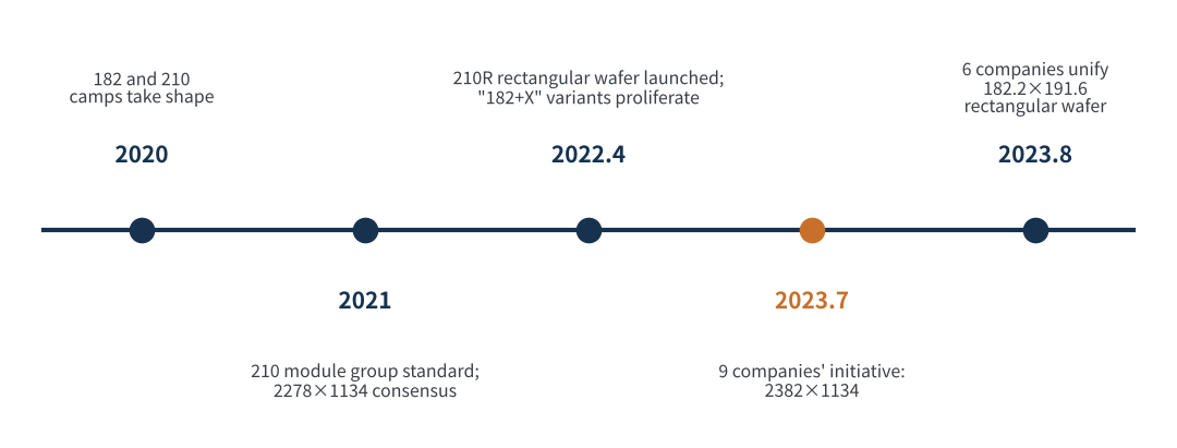
Figure 4 Timeline of wafer and module size convergence
On 7 July 2023, nine module makers (JinkoSolar, LONGi, JA Solar, Trina Solar, Canadian Solar, Tongwei, Astronergy, Risen and DAS Solar) signed the Initiative on Standardization of Rectangular Silicon Wafer Module Dimensions, and agreed to push for the rectangular-wafer module sizes to be included in China Photovoltaic Industry Association standards and to set up a module dimension standardisation working group. Note that this was an "initiative", not a mandatory standard. It took hold because the three boundaries had already squeezed the options into a very small space:
- The boundaries are external: containers, door openings, glass furnaces and mounting systems all predate this size battle, and no module maker can change them.
- The optimum is almost unique: under the constraints of a 1,134 mm width, five pallets per row and compatible holes, the optimal length range is only a dozen or so millimetres, so everyone's calculations naturally converge.
- Deviating carries its own cost: non-standard formats mean pricier materials, custom structures and possible exclusion from tenders; some owners have already written the 182×210 rectangular size directly into module procurement requirements.
In economic terms, this is a classic coordination game: as long as everyone stands at the same point, everyone benefits; whoever deviates alone loses out. So the size battle did not end with one side beating the other, but with everyone stopping together at the "focal point" set by physics and logistics.
06Final thoughts
Once sizes converged, the main battleground of module competition shifted from "making it bigger" back to "making it better": on the same 2382×1134 panel, TOPCon, BC, heterojunction and, in future, tandem technologies compete on efficiency, bifaciality, reliability and LCOE. Size becomes the constant and technology the variable, which is actually good for the whole industry.
Several developments in 2026 bear this out. First, China's mandatory module efficiency standard GB 47834-2026 grades modules by efficiency, and the industry routinely converts its thresholds into power on the 2382×1134 format: 23.2% corresponds to the 630 W bin and 23.5% to the 635 W bin. Second, Huadian's 5 GW framework tender in September explicitly does not restrict cell or module size and only requires efficiency of at least 23.2%, and Longyuan's 6 GW framework tender in October divides lots by conversion efficiency alone. Third, new products all compete on the same "face": Aiko's fourth-generation ABC module reaches 690 W and 25.6% in mass production on 2382×1134, and Canadian Solar's TOPCon 3.0 is rated at up to 670 W and 24.8%. Only once sizes are unified can buyers look at efficiency alone and ignore size.
Of course, this balance is not permanent. Major changes in shipping rules, tracker design or module packaging structures could trigger a new round of "size recalculation". But as long as the container stays the same, the 1,134 mm width and a length of around 2,382 mm are likely to stay with us for many years.
Module size was not decided by anyone; it is the optimum calculated jointly by three hard boundaries: containers, mounting structures and silicon ingots. Standardisation simply wrote that answer down on paper.
Have you run into other situations in module selection or design where you were "boxed in" by the format? We would be glad to hear from you.
References
- China Photovoltaic Industry Association. T/CPIA 0003-2022, Technical requirements for outline dimensions and mounting holes of terrestrial crystalline silicon PV modules.
- Canadian Solar, Risen, JA Solar, JinkoSolar, LONGi, Trina Solar, Tongwei, DAS Solar, Astronergy. Initiative on Standardization of Rectangular Silicon Wafer Module Dimensions, 2023-07-07 (published on Trina Solar's website).
- China Energy News (People's Daily). After nine companies unified module sizes, six more unify wafer sizes, 2023-08-28; IT Home. Six PV companies join again to call for standardised 72-cell rectangular wafer size, 2023-08-18.
- Guangfumen. JA Solar, JinkoSolar and LONGi jointly release 182 module product white paper.
- Cailian Press. Trina Solar calls for unified size standards: 210R rectangular wafer becomes a new cost-reduction path, 2023-03-12.
- Nengyuanquan. Explainer: what is a rectangular wafer, and why has it taken off?
- SolarQuarter. Trina Solar leads industry standardization with golden size modules for all settings, 2023-11-02.
- Sohu. Why 2382×1134 mm won out, 2023-07.
- Economic Observer. New PV rules not yet in force, some modules already out of the race for big orders, 2026-10-17; Sohu report on Longyuan Power's 6 GW module procurement, 2026-10-14; pv magazine. Aiko showcases 690 W back contact solar module with 25.6% efficiency, 2026-06-10.
A PV R&D and technology team with 10+ years of experience | In-depth technical knowledge sharing
Materials · Reliability · Failure Analysis · Standards & Certification · Products · Processes
Exploring AI + PV; collaboration welcome
Disclaimer:
1. Original content reflects the authors' personal views only, is for reference only and does not constitute investment advice.
2. Reposted and cited content is credited to its source, out of respect for original work.
3. Some content was produced with AI assistance (chart generation, data retrieval, concept explanations, etc.); the core framework and key content were written by our technical team and reviewed by people.
4. If anything is inaccurate or infringes your rights, please leave a message or contact us and we will deal with it.